Jumbo Laser Co., LTD. the subsidiary of Syntec Group, specializes in laser and atmospheric plasma applications. Jumbo offers advanced laser demolding systems for wafer recycling and high-precision laser wafer dicing, optimizing semiconductor manufacturing processes. Additionally, its blue light laser welding technology addresses the challenges of processing highly reflective materials, making it ideal for EV battery and motor production, enhancing stability and efficiency.
By integrating Syntec controllers with Leantec robotic arms, Jumbo Laser provides comprehensive smart laser solutions, supporting the automated production lines. With a strong presence in Southeast Asia, Syntec Group has established three subsidiaries and multiple distribution channels, further expanding its APAC operations to strengthen its market influence and accelerate the adoption of smart manufacturing technologies.
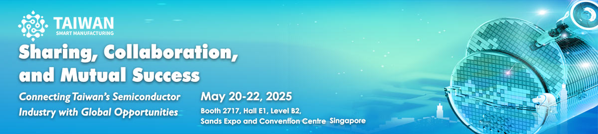
Most wafer dicing processes still rely on diamond blades (mechanical cutting), but they face the following issues:
Laser Dicing – The Technology of the Future
✔ No Burr Formation – High precision with minimal heat-affected zone (HAZ) ensures superior cutting quality.
✔ Non-Contact Processing – No tool wear, reducing consumables and maintenance costs.
Traditional etching and demolding processes rely on chemical acids, which generate large amounts of waste liquid and consume significant water resources, adding to environmental burdens.
Eco-Friendly Laser Technology – A New Solution!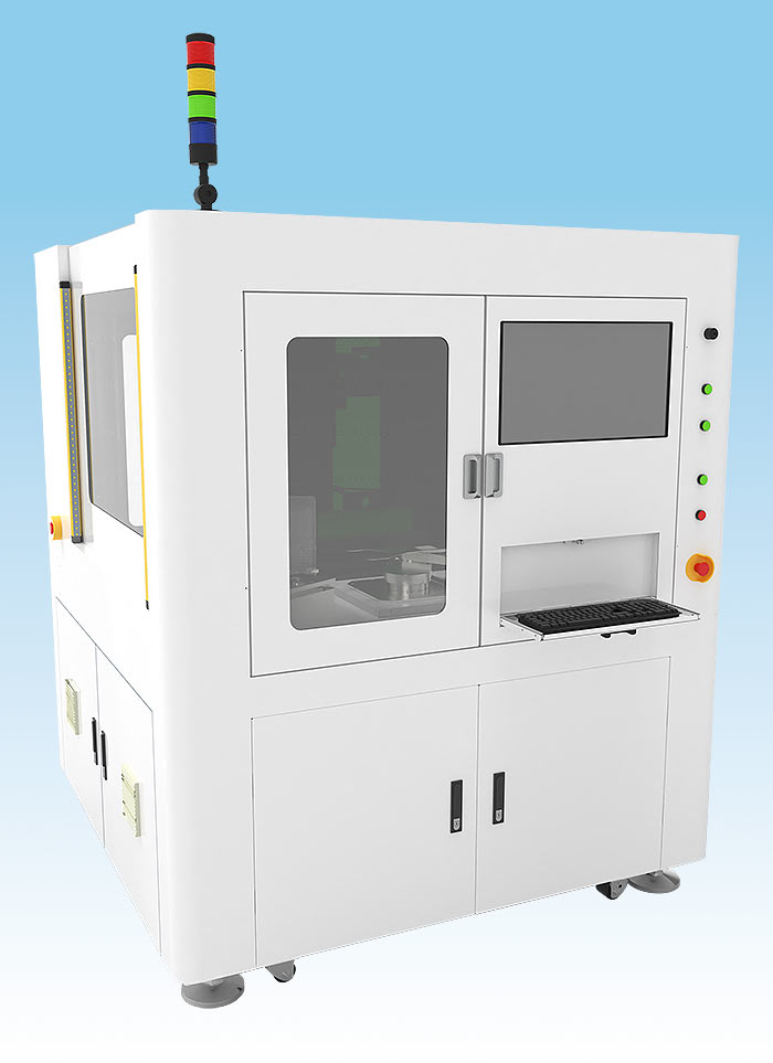
Low Absorption Rate → Energy waste, increased risk of over-welding or false welding.
Large Heat-Affected Zone (HAZ) → Compromised weld quality and reliability.
Blue Laser – The Optimal Solution for Copper Welding
